Facility Name

External users: registration to be carried out only through I-STEM portal
Additional information about sample and analysis details should be filled in the pdf form provided in the I-STEM portal under “DOWNLOAD CSRF”
Internal users (IITB): registration to be carried out only through DRONA portal
Additional information about sample and analysis details should be filled in the pdf form provided here.
.
Category
- Material Characterization » Electrical Characterisation
Booking Details
Facility Management Team and Location
Facility Features, Working Principle and Specifications
Facility Description
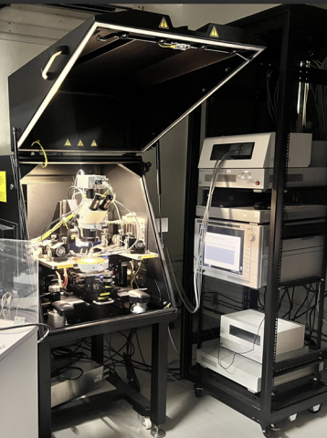
The Power Device Characterization System (PDCS) enables on-wafer and discrete device testing, primarily under high-power conditions.
It supports I–V and C–V measurements using dedicated force and sense probes, requiring four probes for two-terminal devices. The system features automated calibration modules, a display for convenient probing, a vacuum-based chuck for secure sample handling, and a shutter interlock for high-voltage safety. It also offers flexible configurations for two- and three-terminal devices, with gate bias capability provided through a fifth manipulator. The main limitations include the need for separate FORCE and SENSE probes, which increase setup complexity, and the requirement to keep the shutter closed above 42 V in reverse bias due to interlock protection.
NA
Sample Preparation, User Instructions and Precautionary Measures
NA
Si/ Ge/ Metal and Materials that don't vaporize at Room Temp.
Charges for Analytical Services in Different Categories
| IITB Students TA (INR/hr) | IITB students (INR/hr) | IITB Monash students (INR/Hr) | External Academia (INR/hr) | National Labs (INR/hr) | SINE Start up (INR/hr) | Research Park Startup (INR/hr) | Research Park Industry (INR/hr) | Industry (INR/hr) |
| 1600 | 1600 | 1600 +18%GST | 3200 +18%GST | 8000 +18%GST | 8000 +18%GST | 8000 +18%GST | 12000 +18%GST | 16000 +18%GST |
Applications
For electrical measurements of devices
Sample Details
NA
Si/ Ge/ Metal and Materials that don't vaporize at Room Temp.
NA
Atleast >Probe diameter (2,5,7 um)
NA
Samples with Na and K and Outside samples are not allowed
NA
