External users: registration to be carried out only through I-STEM portal
Additional information about sample and analysis details should be filled in the pdf form provided in the I-STEM portal under “DOWNLOAD CSRF”
Internal users (IITB): registration to be carried out only through DRONA portal
Additional information about sample and analysis details should be filled in the pdf form provided here.
.
Category
- Microscopy and Imaging » Electron Microscopy
Booking Details
EDS- Area/Line/Mapping
Facility Management Team and Location
office.saif@iitb.ac.in
0091-22- 2576 7691/2
naresh.ambati@iitb.ac.in
Facility Features, Working Principle and Specifications
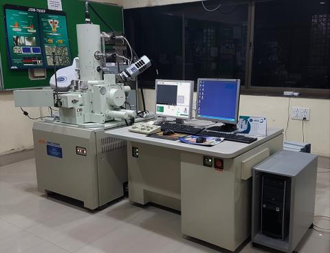
The Jeol field emission scanning electron microscope is a versatile high resolution scanning electron microscope. This Machine combines two proven technologies – an electron column with semi-in-lens objective lens which can provide high resolution imaging by low accelerating voltage and Schottky FEG with strong electrostatic field to induce electron emission. An FEG emitter gives a more coherent beam and its brightness is much higher than the tungsten filament. The instrument is also specialised with Gentle Beam (GB) mode applies a negative voltage to a specimen and decelerates incident electrons just before they irradiate the specimen, thus the resolution is improved at an extremely low accelerating voltage. Thus, this method is suitable for observation of fine structures, especially on low-density materials, non-conductive materials at high magnification with effective detection of low angle backscattered electrons.
- Source: Field emission gun
- SEI Resolution: 1.0nm at 15 kv
1.5nm at 1 kv, in GB mode - Magnification: Low: 25X to 10,000X
High: 100X to 1,000,000X at 4x5 photo size - Accerating Voltage: 0.1 to 30 kv
- Probe Current Range: 1 pA to ≥ 200 nA
Sample Preparation, User Instructions and Precautionary Measures
Sample type that can be analysed: Biological / Composite Material / Thin Film / Crystalline Solid / Metal/Polymer/Ceramic/Composite/Rock/Cement
Sample form that can be analysed: Powder/Pellet/Suspension/Film/Sample on silicon wafer
- Medium for Dispersion Ethanol /Methanol / Water /Iso-propyl alcohol. Any other medium should be provided by the user.
- Dispersion will be done by ultrasonication.
- Kindly mark the edge of the sample to be observed for Cross section.
- Base of the sample should be flat for mounting on sample holder.
- Biological samples will be accepted only after user has done primarily fixation with suitable fixative.
- Sample preparation if any should be done at user end (cutting the sample for CS, freeze fracturing, sample fixation for biological samples, staining of samples, oven drying should be done by the user)
- Cross-section analysis of powdered samples cannot be performed.
- Samples should be in dry form. Hydrated samples must be dried properly before sending.
- The samples should withstand high vacuum (~ 10 -5 Pa). Wet samples cannot be done.
- The bulk sample size should be less than 12.5 mm x 12.5 mm x 10 mm (height)
- For any further query, kindly contact on Email: fegsemlab@iitb.ac.in, Contact: 022 2159 6863
It is preferred that you or a representative who understands the sample and analysis be present on the day of the appointment.
Sample preparation (if any) should be done at the user’s end before the appointment.
The samples must be dry and capable of withstanding ultra-high vacuum conditions.
Charges for Analytical Services in Different Categories
| IITB User | IITB Monash | Academic Institutes | National Lab / R&Ds; Sine | IITB Research Park (Big Industries) /Start-up/MSME (Letter from Research Park/Start-up/MSME required)
| Industry |
|
| No GST | + GST @ 18% | + GST @ 18% | + GST @ 18% | + GST @ 18% | + GST @ 18% |
|
SEM Image (Surface OR Cross Section) | 620 | 620 | 1240 | 3100 | 4650 | 6200 | Per sample |
SEM Image (Surface + Cross Section) | 885 | 885 | 1770 | 4425 | 6637.5 | 8850 | Per sample |
EDS | 175 | 175 | 350 | 875 | 1312.5 | 1750 | Per EDS analysis |
EDS Mapping | 350 | 350 | 700 | 1750 | 2625 | 3500 | Per EDS Mapping analysis |
WDS (Not working) | 350 | 350 | 700 | 1750 | 2625 | 3500 | Per WDS analysis |
WDS Mapping (For 3 element map) | 710 | 710 | 1420 | 3550 | 5325 | 7100 | WDS Mapping for 3 elements |
WDS Mapping (Above 3 element map) | 950 | 950 | 1900 | 4750 | 7125 | 9500 | WDS Mapping for 3 elements |
Applications
- Materials Science/Metallurgy
- Fractography
- Micro drilling and cutting tools
- Dental and medical
- Corrosion
- Polymer Science
- Energy Science/Engg.
- Biological and life sciences
- Semiconductors
- Civil and Earth Sciences
- Nanotechnology
- Ceramics
- Pharmaceuticals
Sample Details
NA
NA
NA
The bulk sample size should be less than 12.5 mm x 12.5 mm x 10 mm (height) and the side opposite the side of interest, should be flat (to enable sample mounting). The smaller the sample height the better.
