External users: registration to be carried out only through I-STEM portal
Additional information about sample and analysis details should be filled in the pdf form provided in the I-STEM portal under “DOWNLOAD CSRF”
Internal users (IITB): registration to be carried out only through DRONA portal
Additional information about sample and analysis details should be filled in the pdf form provided here.
.
Category
- Microscopy and Imaging » Electron Microscopy
Booking Details
Facility Management Team and Location
Facility Features, Working Principle and Specifications
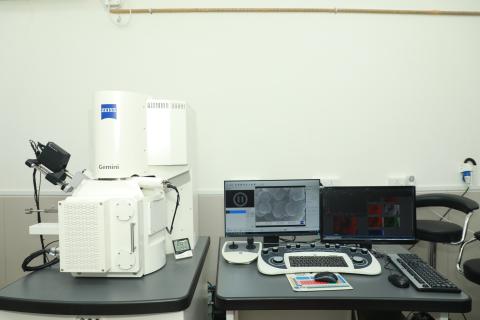
Zeiss Sigma 500 Scanning Electron Microscope (SEM) is a high-performance technique designed for advanced imaging and analytical applications. It features a field emission gun (FEG) for high-resolution imaging, capable of achieving nanometer-scale detail. The Sigma 500 offers a user-friendly interface, fast image acquisition, and superior signal-to-noise ratio. Without the Electron Back scatter Diffraction (EBSD) detector, the instrument focuses on secondary and back scattered electron imaging, along with energy-dispersive X-ray spectroscopy (EDS) for elemental analysis, making it ideal for material characterization and failure analysis. Its modular design allows future upgrades for additional analytical capabilities.
Main features:
• Schottky type field emitter system
• Resolution: 0.8nm at 15 kV; 1.6 nm at 1 kV
• Accelerating voltage: 0.02 to 30 kV
• Beam current configurations: 100nA .
• Electromagnetic beam alignment
• Work distance 0 – 50 mm
• Magnification Range: 10 – 10,00,000x
Sample Preparation, User Instructions and Precautionary Measures
Sample type that can be analyzed: Biological / Composite Material / Thin Film / Crystalline Solid / Metal/Polymer.
Sample form that can be analyzed: Powder/Pellet/Film/Sample on silicon wafer
- Kindly mark the edge of the sample to be observed for Cross section.
- Base of the sample should be flat for mounting on sample holder.
- Biological samples will be accepted only after user has done primarily fixation with suitable fixative.
- Sample preparation if any should be done at user end (cutting the sample for CS, freeze fracturing, sample fixation for biological samples, staining of samples, oven drying should be done by the user)
- Cross-section analysis of powdered samples cannot be performed.
- Samples should be in dry form. Hydrated samples must be dried properly before sending.
- The samples should withstand high vacuum (~ 10 -5 Pa). Wet samples cannot be done.
- The bulk sample size should be less than 12.5 mm x 12.5 mm x 10 mm (height)
- For any further query, kindly contact on Email: fegsem@chem.iitb.ac.in.
Charges for Analytical Services in Different Categories