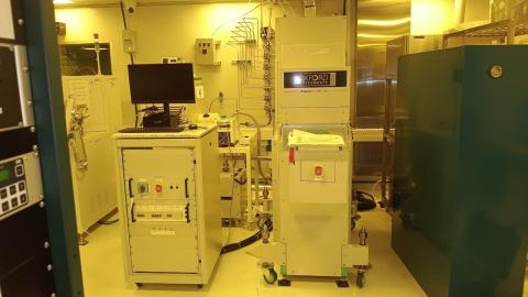
Facility Name

External users: registration to be carried out only through I-STEM portal
Additional information about sample and analysis details should be filled in the pdf form provided in the I-STEM portal under “DOWNLOAD CSRF”
Internal users (IITB): registration to be carried out only through DRONA portal
Additional information about sample and analysis details should be filled in the pdf form provided here.
.
Category
- Fabrication and Processing » Nanofabrication
Booking Details
Facility Management Team and Location
Facility Features, Working Principle and Specifications
Facility Description
Deep RIE or ICP-RIE is a plasma-based etching technique used to create deep, high-aspect-ratio features in substrates such as silicon carbide (SiC), gallium nitride (GaN), and others. It is widely used in processing of GaN-on-SiC devices.
In an ICP (Inductively Coupled Plasma) system, a coil surrounding the process chamber operates at 13.56 MHz to generate an electromagnetic field that ionizes the process gases through inductive coupling, creating a high-density plasma with reactive species necessary for chemical etching. A separate RF power, typically at 2.56 MHz, is applied to the wafer chuck (table) to accelerate ions from the plasma toward the wafer surface, ensuring directional ion bombardment and achieving anisotropic etching profiles. The wafer is held securely during the process using an electrostatic chuck (ESC) to provide stable clamping throughout the etch.
Substrate: GaN on SiC,SiC
Substrate size:0.5”, 1” wafers and small pieces
Temperature of chamber:80C (max, while running the process)
ICP power:3000W( allowed only till 2400W (80%))
RF Power:600W(allowed only till 480W (80%))
Carrier wafer:Sapphire of 4” only with 0.6 mm thickness
Gases connected:SF6,Ar,He,O2,CL2,BCL3,CF4
Sample Preparation, User Instructions and Precautionary Measures
Sample preparation should be on a Sapphire of 4” only with 0.6 mm thickness
Charges for Analytical Services in Different Categories
All charges are in INR / hour
| IITB Students TA | IITB students | IITB Monash students | External Academia | National Labs | SINE Start up | Research Park Startup | Research Park Industry | Industry |
| 2500 | 2500 |
Applications
Sample Details
NA
SiC
SF6,Ar,He,O2,CL2,BCL3,CF4
sample size (≤ 1 inch × 1 inch)
NA
Na and K samples not allowed, Only Ni masks allowed, Au not allowed
NA
