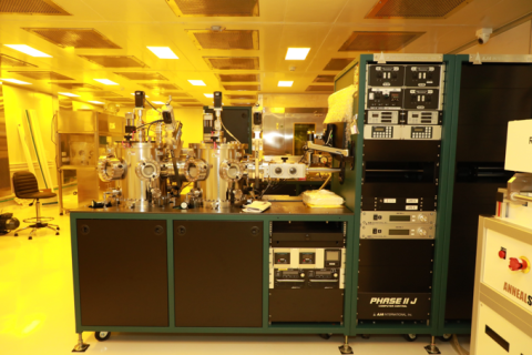
Facility Name

External users: registration to be carried out only through I-STEM portal
Additional information about sample and analysis details should be filled in the pdf form provided in the I-STEM portal under “DOWNLOAD CSRF”
Internal users (IITB): registration to be carried out only through DRONA portal
Additional information about sample and analysis details should be filled in the pdf form provided here.
.
Category
- Fabrication and Processing » Nanofabrication
- Fabrication and Processing » Nanofabrication
Booking Details
Facility Management Team and Location
Facility Features, Working Principle and Specifications
Facility Description
Sputter deposition is a physical vapour deposition (PVD) method of depositing thin films by sputtering material from a 'target', then depositing it onto a 'substrate'. Magnetron sputtering applies a magnetic field around the target in order to energize argon atoms for bombarding the target.
Target Size: 2”
Gases used in the system: O2, Ar, PN2
Substrates used: Si,
Substrate size: Small samples, 2” and 4” diameter wafer.
Magnetic targets allowed
Sample Preparation, User Instructions and Precautionary Measures
NA
NA
Charges for Analytical Services in Different Categories
All charges are in INR
| IITB Students TA | IITB students | IITB Monash students | External Academia | National Labs | SINE Start up | Research Park Startup | Research Park Industry | Industry |
| 2500 | 2500 |
Applications
Thin film deposition, metal contacts
Sample Details
NA
Si
N2, O2
2 inch to 4 inch
2 inch
Na and K not allowed, only magnetic materials are allowed
NA
