Facility Name

External users: registration to be carried out only through I-STEM portal
Additional information about sample and analysis details should be filled in the pdf form provided in the I-STEM portal under “DOWNLOAD CSRF”
Internal users (IITB): registration to be carried out only through DRONA portal
Additional information about sample and analysis details should be filled in the pdf form provided here.
.
Category
- Fabrication and Processing » Microfabrication
- Fabrication and Processing » Microfabrication
Booking Details
Facility Management Team and Location
Facility Features, Working Principle and Specifications
Facility Description
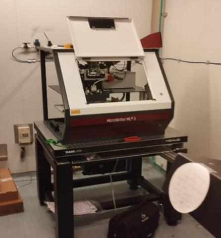
The Microwriter ML 3 is a direct-write photolithography tool which can be used for direct writing on the substrate or mask writing.
The feature sizes (line/space) range from 2 μm (minimum) to 50 μm (maximum) for mask writing, and from 1 μm (minimum) to 50 μm (maximum) for direct writing.
Sample Preparation, User Instructions and Precautionary Measures
NA
NA
Charges for Analytical Services in Different Categories
All charges are in INR/ hour
| IITB Students TA | IITB students | IITB Monash students | External Academia | National Labs | SINE Start up | Research Park Startup | Research Park Industry | Industry |
| 2500 | 2500 | 2500 +18%GST | 5000 +18%GST | 12500 +18%GST | 12500 +18%GST | 12500 +18%GST | 18750 +18%GST | 25000 +18%GST |
Applications
Lithography
Sample Details
Optical resists, S1813, LOR PPR
Si, GaN, Diamond, Quartz
NA
2 inch
NA
Samples with Na and K needs to be mentioned separately for dedicated usage of labware due to contamination issues
NA
