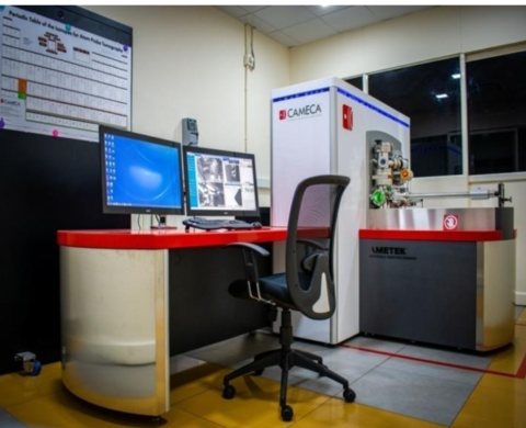
Facility Name

External users: registration to be carried out only through I-STEM portal
Additional information about sample and analysis details should be filled in the pdf form provided in the I-STEM portal under “DOWNLOAD CSRF”
Internal users (IITB): registration to be carried out only through DRONA portal
Additional information about sample and analysis details should be filled in the pdf form provided here.
.
Category
- Material Characterization » Chemical Characterisation
Booking Details
Facility Management Team and Location
Facility Features, Working Principle and Specifications
Facility Description
IIT Madras has established the National Facility for Atom Probe Tomography (NFAPT) which houses a state of art atom probe tomography "Local Electrode Atom Probe (LEAP 5000 XR)" along with "Helios Dual Beam Scanning Electron Microscope with Focused Ion Beam (FIB)" for LEAP sample preparation. IIT Bombay, as a founding partner institute, has a remote terminal for the operation of the instrument and software for the analysis of the data after data acquisition. More details can be found on https://nfapt.iitm.ac.in .
APT is a unique characterization technique that facilitates three-dimensional visualization as well as in‐depth analysis of nano‐scale features at near‐atomic scale resolution (lateral resolution: 0.3-0.5 nm and depth resolution 0.1-0.3 nm). A sharp tip sample is prepared using Focused Ion Beam (FIB). Prepared sample is then cooled and tip is biased at high DC voltage. Due to the sharpness of the tip, high electrostatic field can be generated. This field is sufficient to field evaporate atoms. By applying voltage pulse or laser pulse the field evaporated ions are projected on the position sensitive detector. Time (Time of flight measurement) taken by the ions to reach the detector is noted and the x, y position of the ions is detected. This allows to reconstruct the original position of the evaporated atoms in the analyzed sample.
Sample Preparation, User Instructions and Precautionary Measures
Sample dimensions may vary from thin film samples to small blocks (1 cubic cm) of metallic or non-metallic materials. Porous or soft samples cannot be analyzed using APT.
All information about the material including processing technique and mechanical properties should be provided with the sample.It is recommended to have some prior results from SEM and TEM and a clear idea about the features to be studied before proceeding for Atom Probe Tomography experiment.
The sample preparation will be carried out using FIB at NFAPT, IIT Madras.
Charges for Analytical Services in Different Categories
Charge details for Atom Probe Tomography without GST:
IIT Bombay Users | ||
APT Analysis | Rs. 5,000/- | Per Sample |
Applications
- Interface analysis in magnetostrictive materials
- Grain boundary analysis in metals
- Investigation of phase change separation processes
- Atomic scale characterization of dopants
- Characterization of advanced alloys
- Thin film characterization
- Oxide growth in metals
Sample Details
NA
NA
NA
SOP, Lab Policies and Other Details
Publications
1. High Pressure Torsion Processing of Maraging Steel 250: Microstructure and Mechanical Behaviour Evolution, Kevin Jacob, K., Yadav, D., Dixit, S., Hohenwarter, A. and Jaya, B.N., 2020. Materials Science and Engineering: A, p.140665.
2. Evolution of sub-surface microstructure under linear reciprocating wear of nanostructured bainitic steel, Kritika Singh, SudharmRathore, Aparna Singh, Materials Characterization (2021),Vol 180: 111407.
3.Oriented assembly of Ni-clusters embedded in semi-insulating NiO epitaxial films, Santosh Kumar Yadav, Bhabani Prasad Sahu and SubhabrataDhar, J. Phys. D: Appl. Phys. 55 (2022) 035002 (7pp).
4.Effect of dislocation network on precipitate morphology and deformation behaviour in maraging steels: Modelling and experimental validation,Kevin Jacob, Abhinav Roy, M P Gururajan, Nagamani Jaya Balila
5. Formation of tungsten carbide by focused ion beam process: A route to high magnetic field resilient patterned superconducting nanostructures, H Chakraborti et al. Appl. Phys. Lett. 120,132601 (2022).
6. Revealing a correlation between microstructure, stoichiometry, coherency strains and mechanical behavior of bulk polycrystalline oxide-based age hardened/toughened ceramic alloys, Luv Gurnani and Amartya Mukhopadhyay, Materials Science and Engineering: A 854 (2022) 143810.
7. Micro-mechanisms of failure in nano-structured maraging steels characterised through in situ mechanical tests, Jacob, K., Sahasrabuddhe, H., Hohenwarter, A., Dixit, S. and Jaya, B.N., 2022. Nanotechnology.
8. An experimental study on laser ablation of Ultra-thin SiNx layer of PERC solar cells, Pinal Rana, Durga Prasad Khatri, Anil Kottantharayil, and Deepak Marla. DOI: 10.1177/25165984221129958
9.Understanding the effects of tetrahedral site occupancy by Zn-dopant in Li-NMC towards high voltage compositional-structural-mechanical stability via operando and 3D Atom Probe Tomography studies, A. Sharma, A. H. Pandey, M. K. Jangid, V. Srihari, H. K. Poswal, A. Mukhopadhyay, ACS Appl. Mater. Interfaces, 2023, 15, 1, 782–794.
10. Gupta R., Bhowmick S., Kumar K.C.H., Prasad M.J.N.V. and Pant P, "Transformation of borides in directionally solidified nickel base superalloy and its mechanical response“, Journal of Alloys and Compounds, p.169996, 2023
11. BinitaTongbram, Vidya P. Deviprasad, Amit VitthalKumbhar, SaumyaSengupta, Subhananda Chakrabarti, "Formation of strain reduced In0.54Al0.34Ga0.12As layer of vertically coupled QDs arrays for O-band telecom single photon sources" Journal of Alloys and Compounds , 960, 17061, 2023
12. Vivek Kumar Singh, DebarajSahoo, MurugaiyanAmirthalingam, Shyamprasad Karagadde, Sushil K. Mishra, "Dissolution of the Laves phase and δ-precipitate formation mechanism in additively manufactured Inconel 718 during post printing heat treatments ”Additive Manufacturing ,81, 104021, 2024
13. Pinal Rana, Durga Prasad Khatri, Anil Kottantharayil, Deepak Marla, " Laser ablation of thin SiNx layer coated on silicon wafer—evaluation of process performance for PERC solar cell application", 2024 ,Semicond. Sci. Technol. 39 065003
