.
Category
- Diffraction » X-ray Diffraction
Booking Details
Facility Management Team and Location
Prof. MJNV Prasad
Prof. T R S Prasanna
Prof. Sushil Mishra
Prof. Arindam Sarkar
Prof. Subramaniam Chandramouli
Facility Features, Working Principle and Specifications
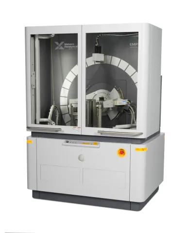
Facility Description
x- ray Diffraction(XRD ) is a versatile non -destructive analytical technique used to analyze physical properties such as phase composition , crystal stucture and orientation of powder solid samples.
Phase identication can be performed by comparing x-ray diffraction patterns obtained from unkmown samples to patterns in reference database.
X-ray Diffraction is the result of constructive interference between x rays and a crystalline sample.
The wavelength of the x-rays used is of the same order of magnitude of the distance between the atoms in a crystalline lattice.
This gives rise to a diffraction pattern that can be analysed by applying the Bragg’s Law (nλ=2dsinθ)which is used in the measurement of crystal and their phases.
X-ray tube: Cu; long fine focus; spinner stage
Pixcel 1D detector with prefix interface
X’pert highscore plus; reflectivity software; easysaxs software
Instructions for Registration, Sample Preparation, User Instructions and Precautionary Measures
- A maximum of six samples will be accepted at a time.
- Only One registration will accepted at a time.
- Maximum two samples will be accepted for half an hour sample scan.
- Collect the samples and the XRD results within 30 days of your registration.
- If user will not collect samples within 30 days then lab person will not responsible for missed samples
Please follow the sample preparation methods below, according to the nature of your analysis.
For Powder XRD
Samples should be submitted in the form of fine powder (preferably less than 10 μm) to completely fill the rectangular cavity of the sample holder of dimension of 0.6 cm3.
i.e. l = 2 cm, b = 1.5cm, h = 0.2 cm.
For Pallet Samples, the sample should have diameter of 2 cm and height 1 cm (maximum).
For Thin Film XRD and GIXRD
Sample size should be minimum 5 cm ´ 2.5 cm.
For SAXS
Details will be provided upon consultation.
Charges for Analytical Services in Different Categories
Applications
- Phase Identification of unknown crystalline materials.
- Characterization of crystalline materials.
- Determination of crystal structures using Rietveld refinement.
- Thin film characterization.
- SAXS method is useful for the structural characterization of nanomaterials. The samples may be solid objects, powders, gels or liquid dispersions, and they may be amorphous, crystalline or semi-crystalline.
- Complete Functional system for Phase Analysis & Crystallography.
- Thin film attachment (GIXRD) & reflectivity measurements.
- Small angle and wide angle X-ray scattering (SAXS/WAXS) measurements & accessories for solids, composites as well as powder as per technical specifications.
Sample Details
SOP, Lab Policies and Other Details
Publications
(1) Jayant K. Dewangan,a Nandita Basub and Mithun Chowdhury *a Cationic surfactant-directed structural control of NaCl crystals from evaporating sessile Droplets. https://pubs.rsc.org/en/content/articlelanding/2022/sm/d1sm01357b
(2) Kartikay, P., Sadhukhan, D., Yella, A., & Mallick, S. (2021). Enhanced charge transport in low temperature carbon-based nip perovskite solar cells with NiOx-CNT hole transport material. Solar Energy Materials and Solar Cells, 230, 111241.
https://doi.org/10.1016/j.solmat.2021.111241
(3). R. Biswas, S. Vitta, T. Dasgupta, Influence of zinc content and grain size on enhanced thermoelectric performance of optimally doped ZnSb, Mater. Res. Bull. 149 (2022) 111702. https://doi.org/10.1016/j.materresbull.2021.111702.
(4). R. Biswas, V. Srihari, S. Vitta, T. Dasgupta, Vacancy induced anomalies in the electrical transport properties of Ag-doped Zn1-xCdxSb (x=0.375) solid solutions, Appl. Phys. Lett. 120 (2022) 032102. https://doi.org/10.1063/5.0077175.
(5)Laxmi, Dinesh Kabra, Origin of Contrasting Emission Spectrum of Bromide versus Iodide Layered Perovskite Semiconductors https://doi.org/10.1021/acs.jpclett.2c00362
