.
Category
- Microscopy and Imaging » Electron Microscopy
Booking Details
Facility Management Team and Location
Facility Features, Working Principle and Specifications
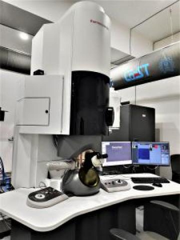
Facility Description
The transmission electron microscope is a 300kV high-resolution microscope with a field emission gun and excellent analytical performance. This facility is used for analysis of elemental composition by energy dispersive spectroscopy, diffraction for crystal structure determination and crystallographic studies.
Specifications
- Point resolution – 0.2 nm for TEM, 0.12 nm for STEM
- Information limit – 0.18 nm
- Minimum Brightness – 9.88 x 10⁷ A/m2srV
- EDS energy resolution at Mn – 125 eV
- Maximum spot drift – 0.45 nm/min
Instructions for Registration, Sample Preparation, User Instructions and Precautionary Measures
Register Through Drona, data will be provided in CD after completion of slot
Powder sample should be sonicated properly and should not agglomerate
Sample Preparation Guidelines
- Sample preparation is to be done by the user.
- Powder sample should be dry and should not be beam sensitive.
- Bulk sample should be a circular 3 mm diameter disk.
Charges for Analytical Services in Different Categories
| User Type | Charges per hour |
| IIT Bombay TAs on Specific Instruments | 200 |
| IIT Bombay Internal Users | 1000 |
| Other Academic Institute | 2000+ 18 % GST |
| National Labs | 4000 +18% GST |
| Industry/Non-Government Entity | 8000 + 18% GST |
| Start-up (SINE incubation) | 5000 + 18% GST |
| Monash IIT Bombay | 1000 + 18% GST |
| SAARCS Countries & African Counties(low-Income Countries) | Academic ₹ 5000 + 18% GST Industry ₹ 10000 + 18% GST |
| For Other Countries | Academic ₹ 10000 + 18% GST Industry ₹ 20000 + 18% GST |
| Cu Grid / Lacey Grid | ₹ 500/- (per grid) |
Applications
Deformation in Metals: Deformation in metals involves changes in the shape or size of a metal object due to the application of an external force. It can occur through various mechanisms such as slip, twinning, or grain boundary movement.
Nano Science/Nano Technology: Nano science and nanotechnology deal with the study and application of extremely small things, typically on the scale of nanometers. This field encompasses various disciplines such as chemistry, biology, physics, and engineering.
Thin Films: Thin films are layers of material ranging from fractions of a nanometer to several micrometers in thickness. They are used in various applications including electronics, optics, and coatings.
Energy Science/Engineering: Energy science and engineering focus on the development of technologies for energy production, conversion, and storage. This includes renewable energy sources, batteries, fuel cells, and energy-efficient systems.
Chemical Composition and Quantification (TEM): Transmission Electron Microscopy (TEM) is used to determine the chemical composition and quantify elements in materials at the atomic level. It provides high-resolution imaging and analytical capabilities.
Elemental Mapping (STEM): Scanning Transmission Electron Microscopy (STEM) is used for elemental mapping to visualize the distribution of elements within a sample. This technique combines imaging with spectroscopy for detailed analysis.
Orientation Mapping (A-Star): Orientation mapping using the A-Star technique involves determining the crystallographic orientation of grains in a material. This is done using advanced electron diffraction methods such as 4D-STEM, which provides high precision and resolution.
Sample Details
Sample Preparation Guidelines
- 3 mm diameter copper grid
- 3 mm diameter bulk sample (Metal/Ceramic)
- FIB Lamella
SOP, Lab Policies and Other Details
Publications
Research References
- R. Tripathi et al. ACS Appl. Nano Mater. 2022, 5, 12, 17767–17782
- P. Gandharapu et al. Clean Technologies and Environmental Policy. 2023
- Vaibhav Verma et al. Carbon, Volume 209, 5 June 2023, 118007
- B.S Kumar et al. Adv. Energy Mater. 2023, 2204407
- Anagha Pradeep et al. Carbon Volume 201, 5 January 2023, Pages 1-11
- I Biswas et al. Chem. Commun., 2023, 59, 4332-4335
- B S Kumar et al. Chem. Mater. 2022, 34, 23, 10470–10483
- Kankona Singha Roy et al., ACS Appl. Mater. Interfaces, 13(8) (2021) 9897-9907
- Anagha Pradeep et al., Elec. Acta, 362 (2020) 137122
- P. Manikandan et al., MMTA, (2021) https://doi.org/10.1007/s11661-021-06337-y
- Agrawal et al., MMTA, 52 (2021) 1465-1476
- Saurabh Kumar et al. Mater. Charac., 2023, 199, 112822
- Aditya Prakash et al., IJP, 2023
- Saurabh Kumar et al., MMTA, 2023, 54A, 1236-1251
- Soudip Basu et al., Mater. Charac., 2023, 197, 112704
- Sanjay Manda et al., MMTA, 2023, 54A, 562-576
- A. Sarkar et al., Mater. Charac., 2023, 194, 112426, 1-15