Facility Name

External users: registration to be carried out only through I-STEM portal
Additional information about sample and analysis details should be filled in the pdf form provided in the I-STEM portal under “DOWNLOAD CSRF”
Internal users (IITB): registration to be carried out only through DRONA portal
Additional information about sample and analysis details should be filled in the pdf form provided here.
.
Category
- Material Characterization » Electrical Characterisation
Booking Details
Low temperature mode
Facility Management Team and Location
bala.ramanathan@iitb.ac.in
022 - 2576-7808
Prof. R O Dusane
Prof. Subhananda Chakrabarti
Prof. Subhabrata Dhar
Facility Features, Working Principle and Specifications
- The versatile Hall Measurement System employs an AC magnetic field for measuring low mobilities down to 0.001 cm2/V.s, much lower than ever possible using traditional DC field Hall measurement techniques.
- The system also has an unusually high resistance option to measure samples with resistance as high as 200 GΩ in van der Pauw geometry.
- Measurement of low mobilities down to 0.001 cm2/v.s, much lower than ever possible using traditional DC field hall measurement techniques.
- High resistance option to measure samples with resistance as high as 200GΩ in van der Pauw geometry.
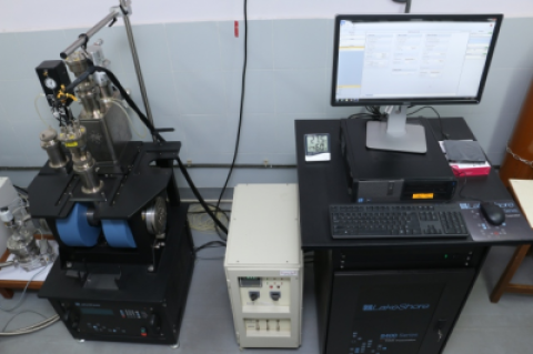
LakeShore Model 8404 AC/DC Hall Effect Measurement System (HMS) can provide a full range of Hall measurements using van der Pauw or Hall probe sample geometries. Options include high resistance and low resistance samples, low mobility samples and variable temperature measurement.
DC Field measurements :
Resistance range: 0.5 mΩ to 200 GΩ
AC Field measurements :
Capable of measuring mobility's down to 0.001 cm2/V.s
Low temperature option :
Variable Temperature assembly (temperature range 15 K to 350 K)
Sample Preparation, User Instructions and Precautionary Measures
It is desirable to have samples of approximate size (8 mm x 8 mm) and thickness 1- 2 mm. Any sample shape is acceptable but the minimum and maximum size should be 5 mm and 15 mm, respectively.
Please note that the HMS Facility provides only indium soldering and conductive silver paint for van der pauw contacts to the samples.
For the first time measurement on a pellet type or solution casted samples, the user must contact the HMS Technical Staff (hms@iitb.ac.in), before registering for a slot. The user should fix up a mutually convenient time to check if it is possible to make point contacts with the available facilities. In case it is not possible to make such point contacts, it will be the responsibility of the user to come prepared for a HMS slot, with four van der pauw contacts of ~ 1 mm size at the periphery of the sample, using suitable metals, like, aluminium or gold, etc., which make ohmic contact to their material.
Charges for Analytical Services in Different Categories
For Internal User:
Rs. 300 per slot (3 Hours) for internal users. Please note that low temperature measurements run for longer duration and will be pro-rated as per above charges.
For External Users:
Charges per sample (maximum time 1 hour)
Industry: Rs. 3,000/- *
National labs/R&D Institutions: Rs. 2,000/-*
University/Academic Institutions: Rs. 500/-* (*GST extra)
For samples requiring more than one hour of analysis, there will be 50% extra charge per hour.
Applications
- The 8400 Series HMS combines the best of both DC and AC field Hall measurement methodologies to facilitate the broadest range of research applications. Optional variable temperature modules and measurement platforms extend the utility HMS to meet the specific needs for a large variety of applications.
- Solar cells: OPVs, a: Si, μ-Si, CdTe, CuInGaSe (CIGS)
- Organic electronics: OTFTs, Pentacene, Chalcogenides, OLED
- Transparent conducting oxides: InSnO (ITO), ZnO, GaZnO, InGaZnO (IGZO)
- III-V semiconductors: InP, InSb, InAs, GaN, GaP, GaSb, AIN based devices, high electron mobility transistors (HEMTs) and heterojunction bipolar transistors
- II-VI semiconductors: CdS, CdSe, ZnS, ZnSe, ZnTe, HgCdTe
- Elemental semiconductors: Ge, Si on insulator devices (SOI), SiC, doped diamond SiGe based devices: HBTs and FETs
- Dilute magnetic semiconductors: LGaMnAs, MnZnO
- Other conducting materials: Metal oxides, Organic and inorganic conductors
- High temperature superconductors
Sample Details
SOP, Lab Policies and Other Details
Publications
1. “X-ray absorption study of defects in reactively sputtered GaN films displaying large variation of conductivity”, M. Monish, C. Nayak, D. S. Sutar, S. N. Jha, D. Bhattacharyya, S. S. Major, Semicond. Sci. Technol., 36(2021), 075019.
2. “A large area flexible p-type transparent conducting CuS ultrathin films generated at liquid-liquid interface”, S. S. Pathak, L. S. Panchakarla, Applied Materials Today, 24(2021), 101152.
3. “Structural, electrical and luminescence properties of (0001) ZnO epitaxial layers grown on c-GaN/sapphire templates by pulsed laser deposition technique”, Simran, S.K. Yadav, S. Dhar, J. Appl. Phys., 131(2022), 015302.
4. M. Mishra, R Saha, L. Tyagi, S. Sushama, S.K. panday, S. Chakrabarti, “Investigation of phosphorus-doping of MgZnO thin films using efficient spin-on dopant process”, Journal of luminescence, 257, 119748 (2023).
5. M. Mishra, S Bhowmick, R Saha, SK Pandey, S Chakrabarti, “Temperature induced conductivity reversal in ZnO thin films”, Proc. SPIE 12422, Oxide-based Materials and Devices XIV, 124220S (2023).
