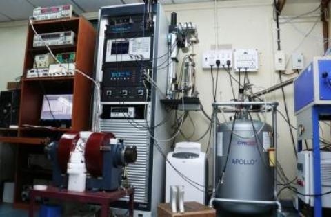
Facility Name

External users: registration to be carried out only through I-STEM portal
Additional information about sample and analysis details should be filled in the pdf form provided in the I-STEM portal under “DOWNLOAD CSRF”
Internal users (IITB): registration to be carried out only through DRONA portal
Additional information about sample and analysis details should be filled in the pdf form provided here.
Make
Novocontrol Technologies
Model
Germany, Concept 80
Facility Status
Working
Facility Management Division
Centre for Sophisticated Instruments and Facilities (CSIF)
.
Category
- Material Characterization » Electrical Characterisation
Booking Details
Slot Booking Link
Booking available for
Internal and External Both
Available Equipment/ Mode of use
Low/high temperature (-150°C to 900°C)
magnetodielectric measurements
piezoelectric measurements
ferroelectric loop measurements.
magnetodielectric measurements
piezoelectric measurements
ferroelectric loop measurements.
Facility Management Team and Location
Facility In Charge
Prof. Prasanna Kumar S Mural
Facility Operator
Ms. Ruchita Vadera
bds@iitb.ac.in
Facility Management Members
Prof. Ajay S. Panwar (HoD, MEMS, Ex-officio member)
Prof. Triratna P. Muneshwar
Prof. Abhijeet L. Sangle
Prof. Jyoti Seth
Prof. Srinivasan Ramakrishnan
Prof. Sankara Sarma V. Tatiparti
Department
Metallurgical Engineering & Materials Science (MEMS)
Lab Email ID
bds@iitb.ac.in
Facility Location
Room No. G003, Ground floor, Dept. of Metallurgical Engg. and Materials Science
Lab Phone No
022-2576-4634
Facility Features, Working Principle and Specifications
Features Working Principle
- It has two separate analyzers:
- From 3MHz to 20MHz working on gain phase measurement method
- From 1MHz to 3GHz working on coaxial line reflectometry method.
- Permittivity, modulus, conductivity (AC), specific resistance (resistivity), tan δ, capacity, impedance, admittance, inductivity, measured temperature, measured time, measured AC volt, measured DC volt, measured AC current, measured DC current.
- Magneto dielectric measurement (For bulk and thin film sample)
- P-E loop measurement (For bulk and thin film samples)
- Piezoelectric measurement (only for bulk sample)
Sample Preparation, User Instructions and Precautionary Measures
Instruction for Sample Preparation
- Sample should be well polished and having smooth surface.
- Maximum of six samples will be accepted at a time for room temperature.
- Maximum of two samples will be accepted at a time with temperature measurement.
- Maximum sample dimension should be diameter of 3 cm and thickness 0.3 cm for Low frequency, and diameter 1 cm and 0.2 cm thickness for RF
- After applying silver paste (Conducting coating) to ceramics samples it should be heated at 150oC at least for one hour.
- User has to bring liquid nitrogen.
- Only one registration will be accepted at a time.
User Instructions and Precautionary Measures
- Payment Mode: Payment should be made in advance by a Demand Draft (DD) drawn in favour of “The Registrar, IIT Bombay, P and C Account". The same should be sent to The Convener, Broadband Dielectric Spectrometer central facility, Department of Metallurgical Engineering & Materials Science, IIT Bombay, Powai, Mumbai -400076.
- Appointment: The users will be informed about their date and time-slot by email. If the day and time-slot is not suitable for you, an email request should be sent immediately for an alternate slot
- : Samples are to be submitted at the time of registration or brought along on the date of your appointment for your sample analysis.
Charges for Analytical Services in Different Categories
Usage Charges
| Broadband Dielectric Spectroscoру Facility | IITB internal users | Other Academic Institutes | National Labs | Industries and Consultancу | Start-up (SINE incubation) | Research Park | Monash IIT B | For Other countries | SAARCS countries & African Countries (Low-Income Countries) | |||
| (IITB TAs) | (IITB (nonTAs)) | (Academics) | (Industries) | (Academics) | (Industries) | |||||||
Room temperature (Per Sample) | INR 125 | INR 250 | INR 500 | INR 1250 | INR 2500 | INR 1250 | INR 1875 | INR 250 | INR 1250 | INR 2500 | INR 1250 | INR 2500 |
| With temperature (any number of samples within six hours) | INR 250 | INR 500 | INR 1000 | INR 2500 | INR 5000 | INR 2500 | INR 3750 | INR 500 | INR 2500 | INR 5000 | INR 2500 | INR 5000 |
| With temperature, after Six hours | INR 50/hr | INR 100/hr | INR 200/hr | INR 500/hr | INR 1000/hr | INR 500/hr | INR 750/hr | INR 100/hr | INR 500/hr | INR 1000/hr | INR 500/hr | INR 1000/hr |
Applications
- Polymers, rubbers, liquid crystals, ferroelectrics, ceramics, Dielectric spectra, molecular relaxation and dynamics, glass transition.
- Pharmaceutical applications, characterization of drugs.
- Structural material properties like phase transitions, phase compositions, and crystallization processes
- Semiconductors, organic crystals: charge transport, activation energy, charge mobility.
- Civil engineering, characterization of concrete.
- Pharmaceutical applications, characterization of drugs.
- Structural material properties like phase transitions, phase compositions and crystallization processes
- Semiconductors, organic crystals: charge transport, activation energy, charge mobility.
