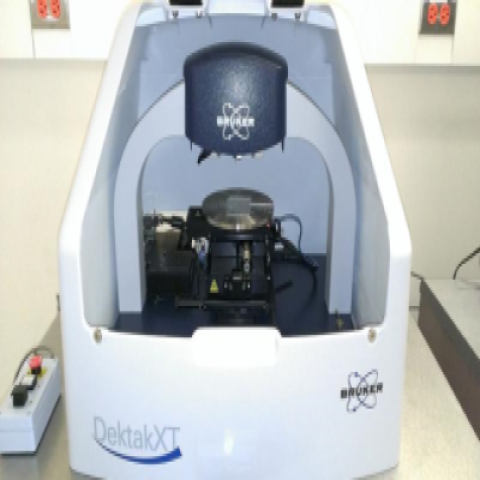
Facility Name

External users: registration to be carried out only through I-STEM portal
Additional information about sample and analysis details should be filled in the pdf form provided in the I-STEM portal under “DOWNLOAD CSRF”
Internal users (IITB): registration to be carried out only through DRONA portal
Additional information about sample and analysis details should be filled in the pdf form provided here.
.
Category
- Material Characterization » Mechanical Characterisation
Booking Details
- Scan Type : Standard Scan, Static Tower scan, Static scan, Map Scan 3D
- Range (vertical) : 6.5 um,65.5 um,524 um,1 mm
- Profile : Hills &Valley
- Stylus Force: 1 mg - 15 mg
- Scan length: scan length between 50 to 55 mm
Facility Management Team and Location
office.saif@iitb.ac.in
0091-22- 2576 7691/2
Facility Features, Working Principle and Specifications
Facility Description
- The DektakXT stylus surface profiler is an advanced thin and thick film step height measurement tool.
Profiling surface topography and waviness. - In addition to taking two-dimensional surface profile measurements, the DektakXT system can produce three-dimensional measurements (3D Mapping) also.
- Stress Measurement for calculating tensile or comprehensive stress on processed wafers.
Stylus profilometers use a probe to detect the surface, physically moving a probe along the surface in order to acquire the surface height. This is done mechanically with a feedback loop that monitors the force from the sample pushing up against the probe as it scans along the surface.
A feedback system is used to keep the arm with a specific amount of torque on it,
known as the ‘setpoint’. The changes in the Z position of the arm holder can then be used to reconstruct the surface. The DektakXT system takes measurements electromechanically by moving a diamond –tipped stylus over the sample surface according to user-programmed scan length, speed and stylus force.
Because a stylus profilometer involves physical movements in X, Y, and Z while maintaining contact with the surface, it is slower than non-contact techniques. The stylus tip size and shape can influence the measurements and limit the lateral resolution.
Sample Preparation, User Instructions and Precautionary Measures
- Substrate Dimension: Provide solid samples Min- 1 cm x 1 cm, Maximum 10 cm x 10 cm (size either in the form square/ rectangular/circular).
- Kindly mark the sample side for the analysis.
- Base of the sample should be flat for mounting on sample holder.
- Samples should be in dry form. Sample preparation if any should be done at user end (cutting the sample).
- Chemical Allowed: No wet chemicals allowed. No sticky and soft sample allowed.
MSDS (Material Safety Data Sheet) should be given along with samples to ensure that samples should not be toxic or hazardous
Charges for Analytical Services in Different Categories
| IIT Bombay Users | IITB-Monash Students | University/ Academic Institute | National Labs/Sine /Research Park IITB (MSME) * Letter from RP Reqd.) | IITB Research Park (Big Industries) / Start-up/MSME (Letter from Research Park/Start-up/MSME required) | Industry
|
|
No GST | + GST @ 18% | + GST @ 18% | + GST @ 18% | + GST @ 18% | + GST @ 18% |
| |
1D or 2D Scan | 260 | 260 | 520 | 1300 | 1950 | 2600 | Per Sample |
3D Scan (Mapping per Hour) | 520 | 520 | 1040 | 2600 | 3900 | 5200 | Mapping per Hour |
Applications
- Solar cell finger width and height
- Thin-film stress calculations
- Transparent films/photoresist thickness, thin and thickfilm measurements
- Microlens height/curvature and V-groove depth analyses
- Roughness studies on machined parts
- Surface quality and defect review
- Metal etch uniformity on wafers
Sample Details
Substrate Dimension: Provide solid samples Min- 1 cm x 1 cm, Maximum 10 cm x 10 cm (size either in the form square/ rectangular/circular).
Kindly mark the sample side for the analysis.
Base of the sample should be flat for mounting on the sample holder.
Samples should be in dry form. Sample preparation if any should be done at user end (cutting the sample).
Chemical Allowed: No wet chemicals allowed. No sticky and soft samples allowed.
MSDS (Material Safety Data Sheet) should be given along with samples to ensure that samples should not be toxic or hazardous.
