Facility Name

External users: registration to be carried out only through I-STEM portal
Additional information about sample and analysis details should be filled in the pdf form provided in the I-STEM portal under “DOWNLOAD CSRF”
Internal users (IITB): registration to be carried out only through DRONA portal
Additional information about sample and analysis details should be filled in the pdf form provided here.
.
Category
- Fabrication and Processing » Nanofabrication
Booking Details
Facility Management Team and Location
Facility Features, Working Principle and Specifications
Facility Description
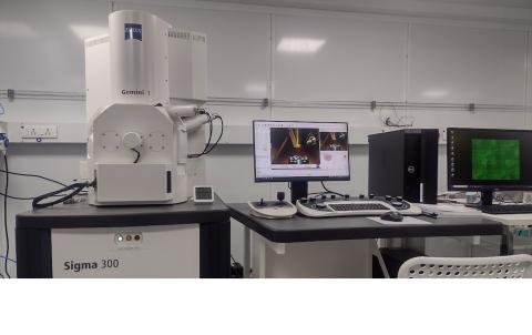
Zeiss sigma 300 SEM and NPGS pattern generation software are coupled together to make an Electron Beam Lithography system. Typically small samples of about 1 cm x 1 cm are handled. The facility is not for full wafer writing. The user will have to learn the basics of the NPGS system and write their own pattern using integrated QCAD software. User needs to be familiar with basic features of CAD systems and preparing clean DXF files with layers.
Note: The system is based on the following :
- Zeiss Sigma 300 FE SEM https://www.zeiss.com/microscopy/en/products/sem-fib-sem/sem/sigma.html
- NPGS v9 external pattern generator https://www.jcnabity.com/
- We do not have metallization/dry or wet etching/gas injection write capabilities. The facility offers pattern writing on electron beam compatible resists and developing. Subsequent processing steps are to be done by the user separately.
Electron Beam sensitive resist (typically PMMA, HSQ) are coated on the sample using a spin coating system. The electron beam is programmed to write the desired pattern on the substrate using specified exposure doses. Pattern is then developed in suitable developer solution for the next phase of processing.
Sample Preparation, User Instructions and Precautionary Measures
Samples should be within 10 mm x 10 mm in size. The maximum writing field is generally 1 mm x 1 mm
To be added
Charges for Analytical Services in Different Categories
| Electron Beam Lithography System at Physics | ||
| Sr. No | Category | Instrument usage charges (per 3 hour slot) in INR |
| 1. | IITB Students | 500 |
| 2. | IITB Students (Facility TAs) | 250 |
| 3. | IITB-Monash Students | 500 + 18% GST |
| 4. | Other Academic Institutes | 1000 + 18% GST |
| 5. | National Labs | 2500 + 18% GST |
| 6. | SINE (Letter from SINE required) | 2500 + 18% GST |
| 7. | Research Park (MSME) (Letter from RP required) | 2500 + 18% GST |
| 8. | Research Park (Big Industry Partners, Letter from RP required) & MSME not associated with RP (appropriate certificate required) | 3750 + 18% GST |
| 9. | Industries | 5000 + 18% GST |
Applications
TBA
Sample Details
Processing chemicals are typically solvents like Acetone, IPA, PMMA (& similar polymers) , MIBK and DI water.
Silicon, Gallium Arsenide, Glass, Sapphire, Quartz . No biological samples.
not applicable
1 cm x 1 cm approx.
na
No biological samples
NA
