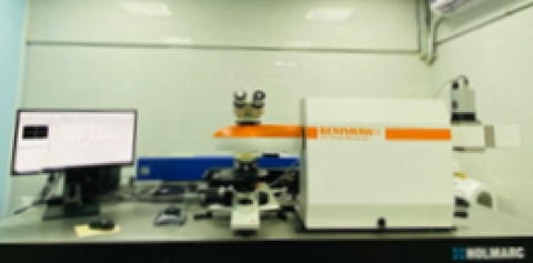
Facility Name

External users: registration to be carried out only through I-STEM portal
Additional information about sample and analysis details should be filled in the pdf form provided in the I-STEM portal under “DOWNLOAD CSRF”
Internal users (IITB): registration to be carried out only through DRONA portal
Additional information about sample and analysis details should be filled in the pdf form provided here.
.
Category
- Spectroscopy and Spectrometry » Raman Spectrometer
Booking Details
Facility Management Team and Location
Facility Features, Working Principle and Specifications
Working Principle:
Light reflected of Raman-active samples irradiated with monochromatic radiation consists of a Raman component having slightly different wavelength as compared to that of the incident radiation. A spectrometer and detector are used to measure intensity of reflected light and it's corresponding wavelength to give us Raman spectrum for the sample.
Features:
Following measurements can be performed using Raman/PL signal-
- Spectral Analysis
- Mapping
- Depth Profiling
Aforementioned measurements can also be performed-
- While varying temperature (Temperature-dependent Analysis)
- While varying degree of polarization / orientation of sample (Polarization-dependent Analysis)
- At specific intervals of time (Time-dependent Analysis)
Specifications:
Spectral Range of System
- Raman - 75 to 4000 cm-1
- PL - 330 to 1600 nm
Motorized Stage
- Maximum travel distance of 110 mm x 75 mm x 25 mm with minimum step size of 50 nm x 50 nm x 10 nm.
- Minimum step-size for mapping is 100 nm.
Range for Temperature-dependent Analysis
- 300K to 12K (using CCR)
- 300K to 1200K (using furnace)
Polarization-dependent Analysis
- Incident light can be polarized as normal, orthogonal or circular.
- Reflected light can be polarized at any angle.
Additional measurements
- Low-wavenumber analysis from 15 cm-1 using LWN filter.
- Fiber-optic probe for analysis of samples which cannot be directly placed on the microscope stage.
Sample Preparation, User Instructions and Precautionary Measures
• Maximum size of sample which can be placed on the microscope stage is 50 mm x 50 mm x 30 mm.
• For temperature-dependent studies sample size should be less than 3 mm x 3 mm x 3 mm.
• If possible, use of coolants/lubricants should be avoided when resizing the samples.
• Sample should remain stable upon exposure to high intensity laser beam.
• For low-temperature analysis, sample must be able to withstand high vacuum conditions.
• For high-temperature analysis, sample should not deform or emit fumes as temperature is increased.
• System’s optical microscope may not be able to acquire data from particles/structures having size less than 100 nanometers.
Charges for Analytical Services in Different Categories
| IIT-B / Monash | Academic Institutes | National Labs / SINE / Research Park (MSME) | Research Park (Big Industry partners) / MSME not associated with Research Park | Industries | ||
| Spectral Analysis - A | 200 | 400 | 800 | 1000 | 1200 | per sample |
| Spectral Analysis - B | 400 | 800 | 1600 | 2000 | 2400 | per sample |
| Spectral Analysis - C | 600 | 1200 | 2400 | 3000 | 3600 | per sample |
| Spectral Analysis - D | 600 | 1200 | 2400 | 3000 | 3600 | per sample |
| PL Mapping | 600 | 1200 | 2400 | 3000 | 3600 | per sample |
| Raman Mapping | 1200 | 2400 | 4800 | 6000 | 7200 | per sample |
| High-Temperature | 800 | 1600 | 3200 | 4000 | 4800 | per sample |
| Low-Temperature | 3000 | 6000 | 12000 | 15000 | 18000 | per sample |
| Polarization-Dependent | 600 | 1200 | 2400 | 3000 | 3600 | per sample |
| Spectral Analysis - A | Uniform samples. Data is to be acquired at any two locations. | |||||
| Spectral Analysis - B | Non-uniform samples. Data is to be acquired at upto five different locations. | |||||
| Spectral Analysis - C | Anything other than Spectral Analysis - A or Spectral Analysis - B. | |||||
| Spectral Analysis - D | Requirement of UV laser / In-situ experiments. | |||||
Charges are excluding 18% GST (wherever applicable). Charges are for estimation purpose only. Charges are for analysis using one particular excitation laser wavelength. | ||||||
Applications
Pharmaceuticals and Cosmetics
Geology and Mineralogy
Carbon Materials
Semiconductors
Life Sciences
Polymer science
Sample Details
--
--
--
--
--
--
SOP, Lab Policies and Other Details
Publications
• Mireja S, Khakhar DV. High β-phase PVDF films formed by uniaxial
compression. Polymer. 2024 Feb 2;293:126665
• Joshi DJ, Jha S, Malek NI, Park TJ, Kailasa SK. Rational design of niobium
carbide MXene quantum dots decorated with arginine for the fluorescence
sensing of superoxide anion in Saccharomyces cerevisiae cells. Sensors and
Actuators B: Chemical. 2024 Apr 1;404:135226
• Patra U, Mujeeb F, Dhar S. Vapor–Liquid–Solid-Mediated Layer-by-Layer
Growth of Stepped-Wedge-Shaped WS2 Microribbons Using the Chemical Vapor
Deposition Technique. Crystal Growth & Design. 2024 Feb 5
• Mandal KK, Singh AK, Kumar B, Shah AP, Vij R, Majumder A, Khunte JJ,
Achanta VG, Kumar A. Emission engineering in monolithically integrated silicon
nitride microring resonators. arXiv preprint arXiv:2401.04963. 2024 Jan 10
