Request form for external booking (Sample and analysis details)
Registration Form for External Users_0.pdf
(130.34 KB)
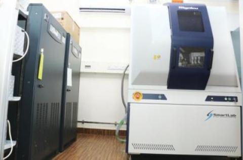
Make
Rigaku diffractometer
Model
Smartlab 9 kW
Facility Status
Not Working
Date of Installation
Facility Management Division
Centre for Sophisticated Instruments and Facilities (CSIF)
.
Category
- Diffraction » X-ray Diffraction
Booking Details
Slot Booking Link
Booking available for
Internal and External Both
Available Equipment/ Mode of use
High resolution microstructural characterization of thin films
Reflectivity
High Resolution powder measurements
In-plane measurements
Reflectivity
High Resolution powder measurements
In-plane measurements
Facility Management Team and Location
Facility In Charge
Prof. Subhabrata Dhar
Facility Operator
Mr. Aniruddha Patil
Facility Management Members
Prof. Subhabrata Dhar
Prof. R Murugavel
Prof. M Senthil Kumar
Prof. Sagar Mitra
Prof. Shaibal K. Sarkar
Prof. Suddhasatta Mahapatra
Department
Physics
Lab Email ID
hrxrd@iitb.ac.in
Facility Location
Room No. 032, Ground Floor, Dept of Physics, IIT Bombay, Powai Mumbai 400076
Lab Phone No
022-2159-6501,
Facility Features, Working Principle and Specifications
Features Working Principle
- High resolution microstructural characterization of thin films
- ω-scan/Rocking curves [RC]
- High resolution ω-2θ using analysers (two bounce or four bound analyser in the diffraction beam optics) [HRω-2θ]
- Reciprocal space mapping [RSM]
- ϕ-scan
- Reflectivity
- Reflectivity measurement [Reflectivity]
- High Resolution powder measurements
- θ-2θ using Johnson mirror [HR-powder]
- Glancing angle diffraction [GLD]
- In-plane measurements
- ϕ-scan/rocking curves [In-RC]
- 2θx-ϕ scan
- High intensity x-ray source (9 kW rotating anode source)i
- Parallel beam optics. (useful for microstructural characterization)
- High resolution goniometer with △θ ▯ 0.0001 Deg as compared to 0.001 Deg for the standard XRD systems.
- In-plane goniometer (useful for in-plane microstructural studies for the thinfilms)
X-ray beam is allowed to fall on the sample and the angles (θ) associated with diffraction maxima [as well as intensity distribution about the maxima] occurring due to different lattice planes are recorded. (θ) is related to the lattice spacing d through Bragg condition 2d Sinθ=nλ where λ is the x-ray wavelength. Information about the lattice structure as well as crystalline quality of a material can be obtained by measuring the angular distribution of intensity about the maxima.
Instructions for Registration, Sample Preparation, User Instructions and Precautionary Measures
Instruction for Sample Preparation
Following type of samples cannot be handled
(i) Health hazardous samples
(ii) Liquid samples
Charges for Analytical Services in Different Categories
Usage Charges
| IITB (internal) | Government Run Universities | External Institute/ Private Universities | Industry | |
| Charges per slot (3 Hours of measurement) | Rs. 500/- | Rs.500/- | Rs. 750/- | Rs. 1500/- |
Applications
- Microstructural characterization of epitaxial films
- Phase determination and texture analysis of polycrystalline samples with higher accuracy.
- Reflectivity measurements: layer thickness, composition, roughness of thinfilms
Sample Details
SOP, Lab Policies and Other Details
Publications
- Jaswant S. Rathore, Rajveer Fandan, Shalini Srivastava, Krista R. Khiangte, Sudipta Das,Udayan Ganguly, Apurba Laha, and Suddhasatta Mahapatra,” Self-Assembled Sn Nanocrystals as the Floating Gate of Nonvolatile Flash Memory”,ACS Appl. Electron. Mater. 2019, 1, 1852−1858
- Rajendra K. Saroj, S.D Kaushik, S.Chopra and S.Dhar,”Influence of Barium doping on structural and magnetic properties on c-ZnO epitaxial layers grown on c-GaN/Sapphire templates”, Thin Solid Films, 691(2019) 137582
- B.K,Barick, S.Deb and S.Dhar,” Generation of light-induced surface current in c-oriented InN epitaxial layers”, Applied Physics A (2019) 125:84
- .Das, D., Saha, J., Panda, D., Tongbram, B., Raut, P. P., Ramavath, R., ... & Chakrabarti, S. (2019). Vertically Coupled Hybrid InAs Sub-Monolayer on InAs Stranski–Krastanov Quantum Dot Heterostructure: Toward Next Generation Broadband IR Detection. IEEE Transactions on Nanotechnology, 19, 76-83.
- .Deviprasad, V. P., Das, D., Tongbram, B., Panda, D., Paul, S., Mondal, S., & Chakrabarti, S. (2019). Spatial optimization of modulation doping in PIP QDIPs: Towards achieving higher operating temperature. IEEE Transactions on Nanotechnology, 19, 247-254.
