Facility Name
External users: registration to be carried out only through I-STEM portal
Additional information about sample and analysis details should be filled in the pdf form provided in the I-STEM portal under “DOWNLOAD CSRF”
Internal users (IITB): registration to be carried out only through DRONA portal
Additional information about sample and analysis details should be filled in the pdf form provided here.
.
Category
- Fabrication and Processing » Microfabrication
Booking Details
Facility Management Team and Location
Facility Features, Working Principle and Specifications
Facility Description
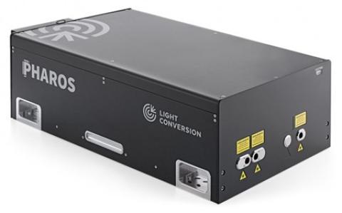
The femtosecond laser system can be used for microfabrication applications for all kinds of materials including metals, non-metals, semiconductors, polymers, and transparent materials. It is equipped with a Pharos Femtosecond Laser, optical system, galvo scanner with an f-theta lens, xyz precision stage and objective lens. This system delivers laser pulses of energy up to 200 mJ, and with pulse durations tuneable from 209 femtoseconds to 10 picoseconds. It operates at 1030 nm and 515 nm wavelengths, with output power of up to 10 W with repetition rates ranging from 1 kHz up to 1 MHz., making it suitable for a wide range of nonlinear and precision applications.
The output beam has a Gaussian profile (M2<1.2), and the beam spot size can be adjusted from 100 microns down to 5 microns using focussing lenses, allowing for fine control over the focal spot size depending on the application. The system is also equipped with a high-speed galvo scanner capable of scanning an area of 5 × 5 cm, enabling flexible beam steering. The use of xyz precision stages allows processing over a wider area.
Femtosecond laser microfabrication is a high-precision technique that leverages ultrashort laser pulses to process materials at the microscale. The laser beam emerging from the femtosecond laser source is first modulated using a combination of beam expanders and focusing optics to achieve a tightly focused spot size ranging from approximately 5 to 100 micrometers, depending on the application and material system. This focused beam is then directed onto the target substrate mounted on a high-precision xyz stage, allowing for controlled patterning in two or three dimensions.
The extremely short pulse duration and high peak intensities ensure that the energy is deposited into the material within a very brief time interval. This ultrafast energy deposition leads to nonlinear absorption mechanisms, such as multiphoton ionization and avalanche ionization, especially in transparent or wide band-gap materials. These mechanisms can induce localized phase transformation, ablation, or even micro-explosions in the focal region, enabling precise removal or modification of material.
Due to the femtosecond pulse duration, there is minimal thermal diffusion to the surrounding material, which significantly reduces the heat-affected zone (HAZ). This thermal confinement is crucial for achieving high spatial resolution and avoiding thermal damage, making it suitable for microstructuring sensitive materials such as polymers, glasses, semiconductors, and biological tissues.
- Power =10 W
- Max. repetition rate=1 MHz
- Pulse width = 205 fs - 10 ps
- Wavelength = 515, 1030 nm
- Beam exit diameter = 3.65 mm
- Focal length = 20 - 120 mm
- Beam spot diameter = 5- 100 μm
Sample Preparation, User Instructions and Precautionary Measures
Charges for Analytical Services in Different Categories
| IIT Bombay |
1000/hr |
| Indian Academia |
2000/hr + 18% GST |
National Lab |
4000/hr + 18% GST
|
Industry and other non-government entities |
8000/hr + 18% GST |
All charges will be calculated based on the total processing time, which includes machine set up time, parameter optimization, and actual processing.
The above charges are exclusive of material costs.
If parameter optimization would require other institute facilities such as microscopy or imaging, additional charges would be incurred as per the facility usage norms.
Applications
- Precision micromachining
- Laser ablation
- Laser shock peening
- Deep hole micro drilling
- Surface texturing
- Microchannels and micropillars
- Precision cutting of metals and non-metals
- Subsurface marking in transparent materials like glass, sapphire, and diamond
- Optical waveguide in transparent materials
- Diamond marking and cutting
Sample Details
All substrates