Facility Name
External users: registration to be carried out only through I-STEM portal
Additional information about sample and analysis details should be filled in the pdf form provided in the I-STEM portal under “DOWNLOAD CSRF”
Internal users (IITB): registration to be carried out only through DRONA portal
Additional information about sample and analysis details should be filled in the pdf form provided here.
.
Category
- Microscopy and Imaging » Force Microscopy
- Material Characterization » Electrical Characterisation
Booking Details
Facility Management Team and Location
Facility Features, Working Principle and Specifications
Facility Description
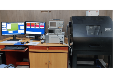
This facility s a technique that uses a AFM tip to measure the topography of a sample surface along with its local electrical conductivity. This facility was installed in Aug 2015 and is widely used to study the electrical properties of materials like semiconductors, nanomaterials, organic electronics etc.
Features:
- Has a maximum scan area of 90x90 μm2 and minimum scan area is around 10 to 30nm. Maximum scan depth is 14μm and minimum can be a few nanometres
- Good external noise isolation
- High speed pulse measurement capability through tip
- The sample preparation is minimum
- It has a maximum Scan Area of 90 x 90 μm2 and minimum scan area determined by tip radius, which is around 10 to 30nm. Maximum Scan Depth is 14μm and minimum can be a few nanometres.
- Good external noise Isolation.
- It can measure localized IV using standard and custom waveforms though nano scale conductive tips.
- High speed pulse measurement capability through tip is also added.
Working Principle:
IThe cAFM facility was installed in Electrical engineering department as a Central Facility as per RIFC norms. The facility is open for all IIT Bombay internal users to meet their research necessities.
The AFM consists of a nanoscale tip mounted on a cantilever that scans over the sample interacting with its force fields. The resulting deflections of the cantilever is converted into a laser beam deflections and it is used to map topography and morphology of samples. Additionally it can measure electrical, magnetic and piezo-electric behaviour of the surface using suitable probes.
Sample Preparation, User Instructions and Precautionary Measures
Preferably samples size should be less than 2cm × 2cm. For CAFM measurements back contact or visible bottom contacts/ pads are required.
Max sample size permitted is 3cm * 3cm * 3cm. For better results, sample should be much smaller than the maximum sample size.
Samples should be thin films, wet and powdered samples are not allowed.
Charges for Analytical Services in Different Categories
S. No. | Category | Charges | GST@ 18% | Total |
| 1. | IITB (TAs) | 500 | No GST | 500 |
| 2. | IITB Students | 1000 | No GST | 1000 |
| 3. | IITB Monash Students | 1000 | 18%GST | 1180 |
| 4. | Academic Institutes | 2000 | 18%GST | 2360 |
| 5. | National Labs | 5000 | 18%GST | 5900 |
| 6. | Sine ( Letter from SINE required) | 5000 | 18%GST | 5900 |
| 7. | Research Park (MSME) (letter from RP required) | 5000 | 18%GST | 5900 |
| 8. | Research park (Big Industry partners -letter from RP required) and MSME not associated with RP (appropriate certificate required) | 7500 | 18%GST | 8850 |
| 9. | Industries | 10,000 | 18%GST | 11800 |
Applications
Material characterization applications including thin dielectric films, nanotubes,conductive polymers, and others Characterize ferroelectric and Piezoelectric materials, temperature control measurements.
Sample Details
All chemicals are allowed
Silicon, ITO, glass, gold, mica, copper sheet etc.
All non toxic gases allowed
Preferably samples size should be less than 2cm × 2cm. For CAFM measurements back contact or visible bottom contacts/ pads are required.
Only dry samples (thin films) are allowed as wet samples may contaminate the AFM tip used for imaging.